If you have been troubleshooting circuit boards for a length of time then it may come as no surprise that many printed circuit boards (PCB) are damaged by surges, spikes and torrents of nasty over-current eruptions coming from the outside.
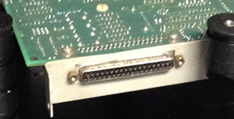
Connector on PCB
Of course, the connectors on the PCB are the interface to that dangerous outside world so it makes sense to use the PCB connectors as a starting place when troubleshooting. This is helpful especially if you have no documentation (i.e. schematics) or know little about the board. Here are some great examples of PCB problems initially detected by testing at the connector level first. The faults were detected by comparing measurements from good boards to bad boards. These examples used a Huntron Tracker and Huntron’s Workstation software for the fault detection but based on the severity of the faults, any decent power-off test instrument would have probably detected differences as well.
Yes, it IS that IC…
This example shows the Huntron Tracker signatures from J11 (which was scanned first) and IC25. The top row of signatures in each image shows each faulty pin in four “Tracker” ranges. The point to note is that the signatures for the faulty pins are the same for the connector AND the integrated circuit IC25. This leads us to believe that they are connected to each other which was verified by checking continuity between the two points.
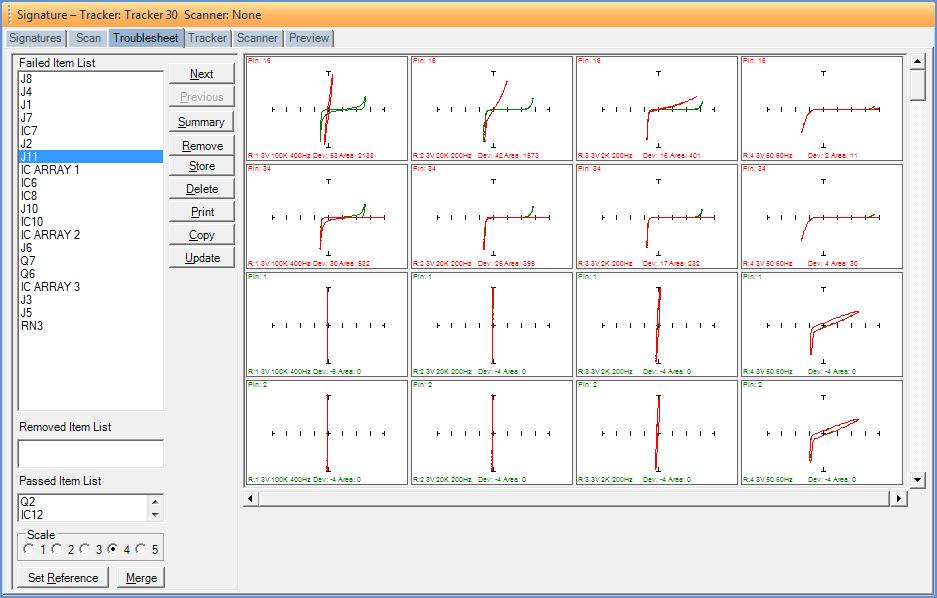
Fault signatures from J11 (click to enlarge)
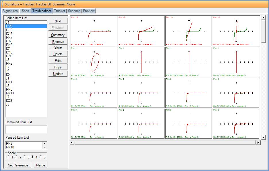
Fault signatures of IC25 (click to enlarge)
Here is an image of the PCB with IC24 and J11 visible. The red arrow indicates the faulty IC pin. The trace from the connector J11 goes only to pin 15 of the IC so we can say with strong confidence that IC25 is the actual problem. This is a relatively complex PCB so it was a relief to be able to spot an issue quickly from the PCB connectors.

Faulty IC on PCB (click to enlarge)
Burns Mark the Spot…
This fault was detected from the connector and using a CAD view and video microscope allowed us to quickly isolate the faulty resistors. Here are the Tracker signatures for two failed resistor NETs on a very complex surface mount technology (SMT) circuit board:
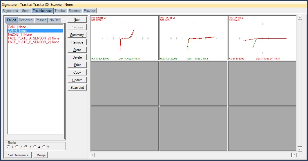
Signature faults from first resistor net (click to enlarge)
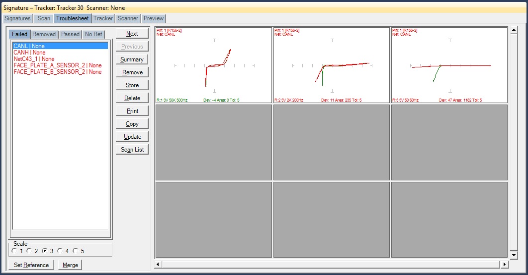
Signature faults from second resistor net (click to enlarge)
Note that the signatures for the two resistor nets are very similar. Using the CAD view data from the PCB layout helped us zero in on the location of the faulty components. Note that both resistors connect to the 25 pin connector close by.
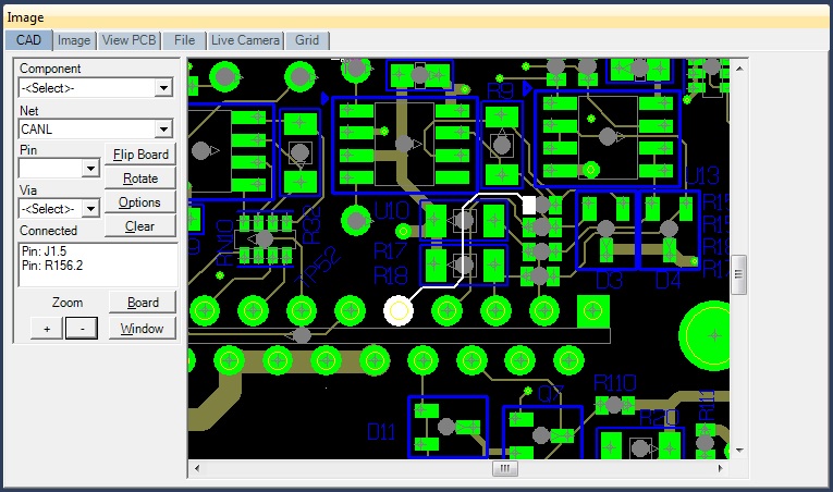
CAD view of first faulty resistor net (click to enlarge)
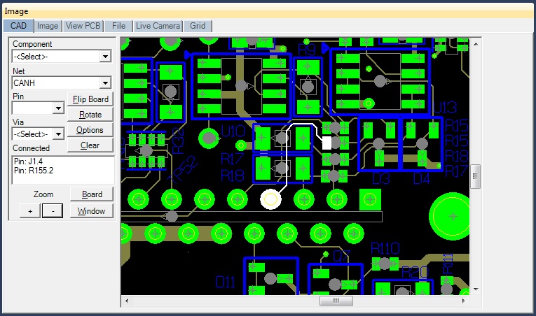
CAD view of second faulty resistor net (click to enlarge)
Breaking out the trusty close-up video camera, we were able to see the burn marks on the two faulty resistors. The damage is somewhat difficult to see but if you compare to the two resistors below you can get an indication on how they should appear.
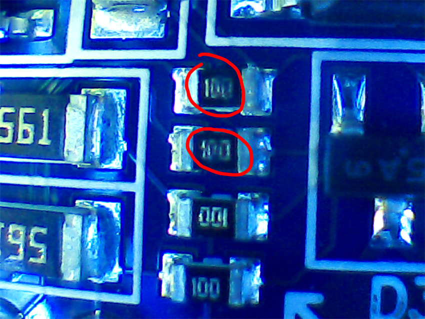
Image of the two faulty burned resistors (click to enlarge)
In conclusion…
While scanning the PCB connectors first may not always lead you to the component faults, it is always an easy and convenient place to start especially if the PCB has a lot of small components that are difficult to probe manually. Connectors are generally much more friendly when it comes to hand probing.
Thanks for reading!