One of the more difficult types of electronic repair tasks is troubleshooting bus structures on complex digital microprocessor based circuit boards. Many identical address and data bus lines share the same electrical characteristics and make the fault finding process a challenge. However, you can use the repeating nature of this digital structure to your advantage.
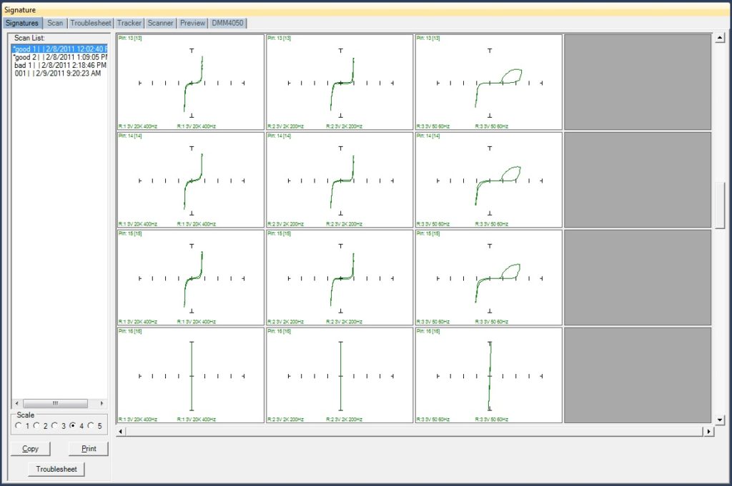
When troubleshooting a complex medical imaging PCB we ran into a situation where we saw many repeating VI signatures because of its digital nature. So when using our Huntron Tracker to capture these signatures we were able to identify repeating patterns that related to specific address lines and data lines. Examine this image to see an example of these repeating patterns.

Note the repeating patterns on the Tracker signatures. The top 3 rows of pins are all of the same type.
The top three rows of signatures are from pins 13,14 and 15 of the tested IC. The bottom row is pin 16 connected to Ground (hence the short circuit indication). These signatures were captured from a known good PCB.
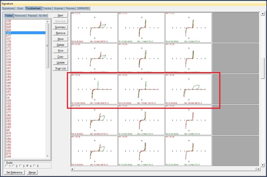
Now examine the same signatures captured from the bad PCB.
Pin 13 is circled with the red box and pins 14 and 15 are below 13. The red signatures are from the bad board and are superimposed over the green good signatures. Pin 13 is important because the red signatures differ significantly from the good signatures in that they are missing the secondary breakdown point on the right side of the signature. While the pin 13 red signatures do not look inherently bad (as in resistive, shorted, open, etc.), they differ from ALL of the similar bus pins that show this secondary breakdown point. This difference gave us cause to take a closer look at this pin of the IC.
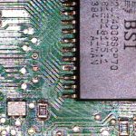
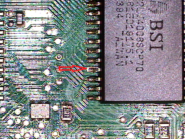
The bad pin 13 is indicated by the arrow. If you look closely, the solder joint on this pin is non-existent and is causing an open connection between pad and pin. With the pin not connected to the solder pad, a change in the electrical nature at this point is created and is reflected in the Tracker signatures.
In conclusion, look for those repeating patterns in measurements when troubleshooting bus circuitry and when you see something out of the ordinary, take a closer look.


