In Troubleshooting a Switching Power Supply – Part 1, we had replaced U1 and CR12 based on the analog signatures from the Huntron Tracker showing them as bad.
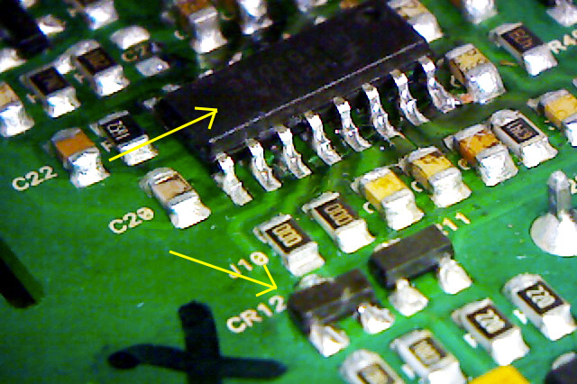
U1 and CR12 (yellow arrows) were replaced
On the rescan, the unit (for practical purposes) passed when compared against our known good reference signatures. There were no catastrophic problems indicated that would make us wary of putting the unit under power. So with a digital multimeter connected to the -12V output, we powered the unit without a load attached for the initial measurements.
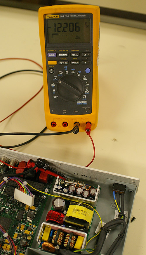
Measuring the -12V output without Load
The +12V, 5V and 3.3V outputs also measured correctly at this point. Next, we connected the load to the power supply and took the same DC measurements (the 3.3V measurement is shown below).
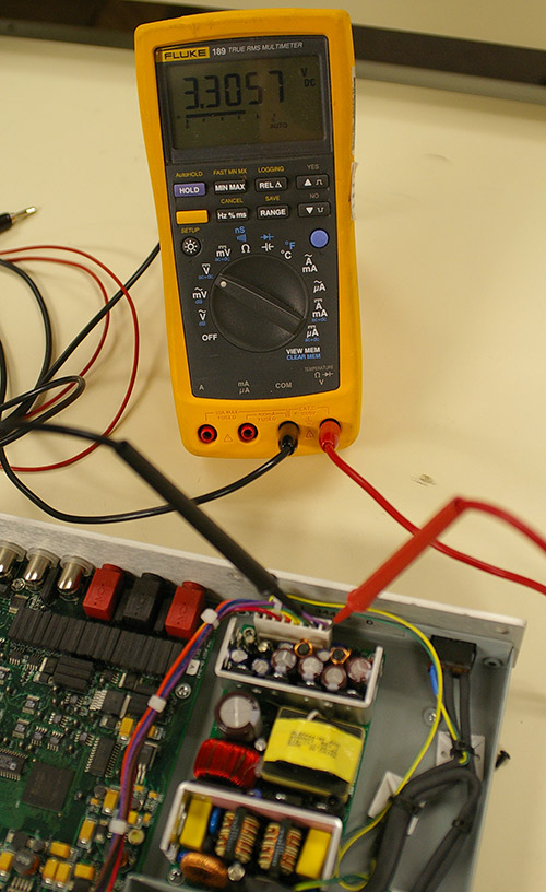
Measuring the 3.3V output with the power supply under load
All of the voltages under load measured correctly. As a final check, the AC voltage was measured at each output to ensure there was no AC ripple on these supply lines. None of the outputs measured above 12mVAC indicating that the voltage filters were in good shape.
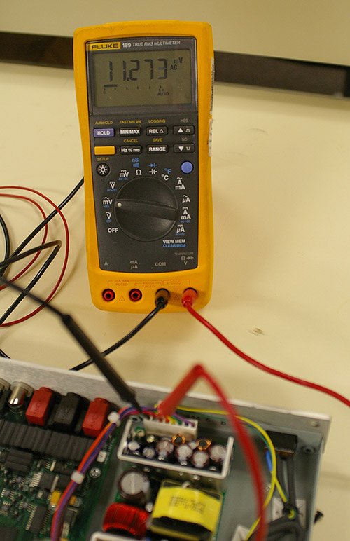
Measuring for AC ripple on the output lines
It appears our repair was successful. We will burn-in the supply in a working assembly to make sure.
So the question is, why did the power supply fail? The damaged circuitry was not in a location that was vulnerable to outside spikes or surges. To answer the question, we went back to the close-up image of the burned diode and took a closer look. It appears that the anode connection of CR12 (pin 3) has a bad solder joint! We did not notice this on first inspection so we were glad to have the image.
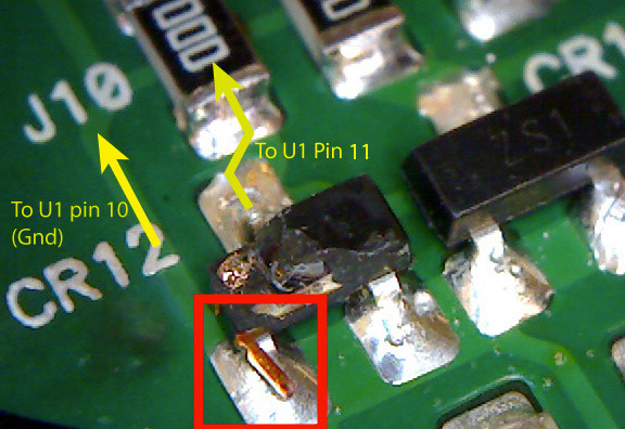
Bad solder joint marked with a red box
At this point there a level of speculation regarding what could happen if the anode pin attached to ground became resistive. Take a look at a basic diagram of the circuit below as a reference.
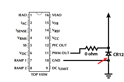
Basic circuit diagram of U1 driver output
It is likely that over time the CR12 solder joint (marked by the red arrow) became more resistive to a point where the control IC U1 was trying to compensate by increasing the level at the Pin 11 driver connection. This conceivably could start to overstress CR12 to a point where it burned. Once it burned and became open to ground the PWM output had no clamping, overstressed and became open (verified by checking pin 11 of the IC out of circuit). Again, this is our opinion but it appears to be a likely scenario. Please add your comments to this post if you have some input on this subject.
Thanks for the visit!
Nicely written articles (Part 1 and 2!). I have shared this with some of my collegues and we had a discussion about the bad solder joint and for the most part agree with your conclusions. How long was the supply in the field before it failed?
Thanks.
Sid
Hi Sid,
Thank you for the nice comment.
As far as we know the power supply was in the field for about 6-7 months. The equipment design does not put a heavy load on the supply so that is why it probably lasted a while.